The Optoelectronics Group News Broadcast
Q&A Session 16:15 - 16:45 on Monday 21st September
This just in: perovskite semiconductors are all the rage as the new and improved material class for solar cells and light emitting diodes (LEDs)!
With just a quick glance around your home you will find a diverse range of objects that are designed to convert electricity to light and other way round: from small displays in your pocket to a solar cell panel on the roof. What makes these optoelectronic devices possible? Meet semiconductors: a class of materials that, when given a boost of energy, will generate light, or – “harvest” the light and convert it to electricity
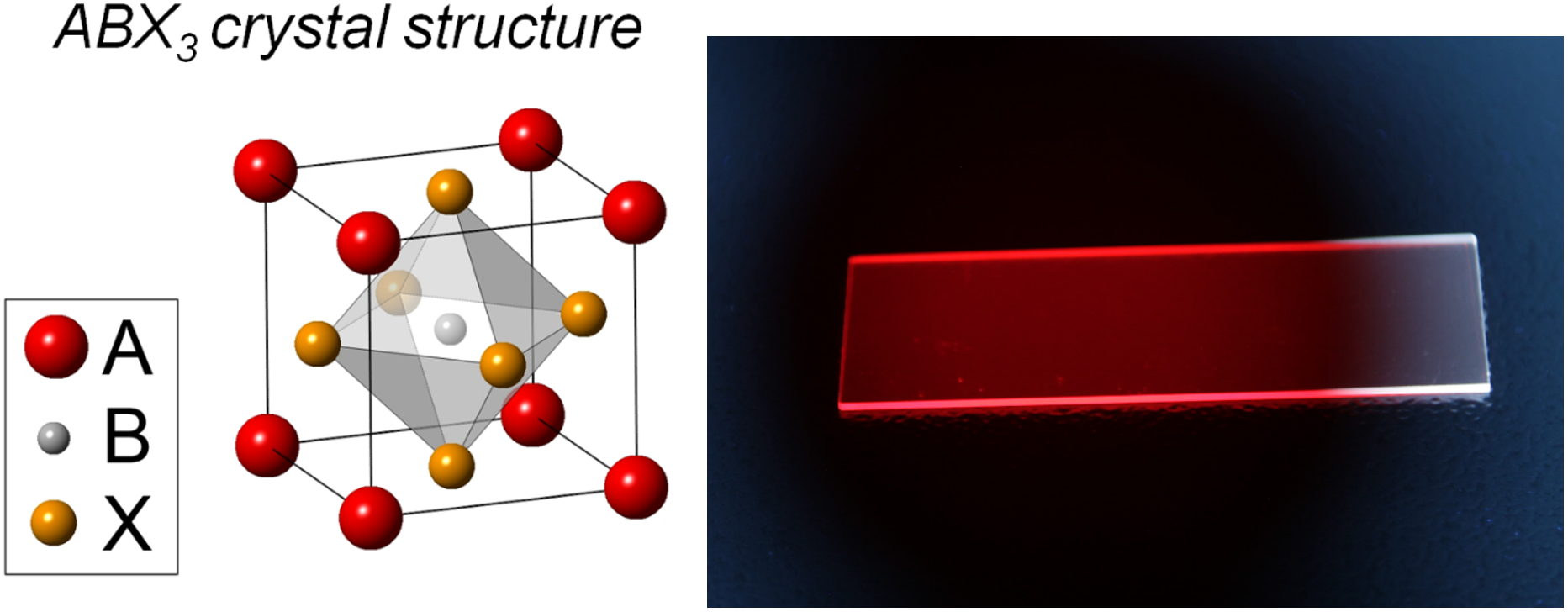
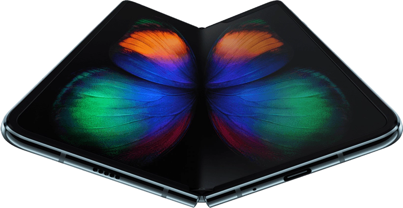
Now, think about the old “brick” bar phone somewhere deep in your parent’s drawer. You probably will not even recognize as a phone. This technology is changing so rapidly because researchers, like us, are constantly investigating new materials that can be lightweight, flexible, and more efficient at operation. Here in the Optoelectronics Group at Cambridge, we study novel materials, such as hybrid organic-inorganic perovskites (Fig 1). These compounds are so efficient, that a perovskite-based device – whether it is a solar cell, or a light emitting diode (LED) – requires only a very thin film of perovskite material, about a 100th of the width of a human hair. These films can be easily imprinted on a flexible substrate – making them lightweight, bendable, and inexpensive. You can now have a smartphone in our back pocket without noticing it, or a portable solar cell on your jacket (Fig. 2) – and we want to make them even better using perovskites!
Research in the Optoelectronics Group focuses on exploring these new materials and fundamentally understanding how they efficiently convert light energy into electricity (vice versa). We work on trying to optimize their performance to produce better light emitting diodes, solar cells and transistors (did you know there are billions of transistors in a single smartphone‽). As researchers, we try to ensure that our processes and fabrication methods are compatible with industrial techniques so that we can more easily transition towards large-scale manufacturing, which make the products you buy at the store (or online) cheaper.
In our event, we will take you on a tour of the synthesis, spectroscopy, characterization, and device testing labs, to show you a day-in-the-life of an optoelectronics researcher. Following the video, we will hold a live, online panel discussion where we can answer your questions. We hope that our presentation will inspire you to learn more about this field – and to consider the amazing new applications these devices could become. And on that matter, how do you think our lab work might positively impact the enormous global challenge of climate change, or the well-being issues emphasized by the COVID pandemic?
Further Information:
Dr Sam Stranks about perovskites revolutionizing photovoltaics @ TeD 2016
Basic info on devices and the physics behind them can be found on this science and engineering popularizing website: www.howstuffworks.com
Feedback:
More detailed feedback can be given here.