Mind the gap! A semiconductor game with the Optoelectronics Group
Look around you and you will find a diverse range of objects that are designed to convert electricity to light and the other way round: from small displays in your pocket to a solar cell panel on the roof. What makes these optoelectronic devices possible? Meet the semiconductors, a class of materials that, when given a boost of energy, are capable of generating light or electricity. Specifically, a certain amount of energy, termed as the band gap, is needed to exchange electrons within a material between the energy levels in a semiconductor. Absorption of light promotes an electron to the higher energy level (let’s call it the “conduction band”) so it can contribute to electric current. The other way round - when we inject electric current into a material (for example, when we plug something in to an outlet) the electrons travel to the conduction band, and then relax to the lower energy state (called the “valence band”), emitting light. Sounds new? Drop in to learn more about just how important the bandgap is to optoelectronic device operation, and feel what it’s like to be an electron in such a material, jumping back and forth across the bandgap!
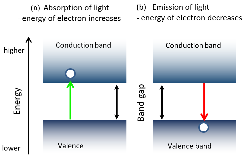
Figure 1: A simplified schematic of semiconductor band structure and transitions related to light
Do you want to know more about our activities? Think about the old “brick” bar phone somewhere in deep in your parent’s drawer. This technology is changing so rapidly because researchers, like us, are constantly investigating new materials that can be lightweight, flexible, and more efficient at operation. Here in the Optoelectronics Group at Cambridge, we study these novel materials, such as hybrid organic-inorganic perovskites (Fig 2). These compounds are so efficient, that a perovskite-based device – whether it is a solar cell, or a light-emitting diode (LED) – requires only a very thin film of perovskite material, about a 100th of the width of a human hair. These films can be easily imprinted on a flexible substrate – making them lightweight, bendable and inexpensive. You can now have a smartphone in our back pocket without noticing it, or a portable solar cell on your jacket (Fig. 3) – and we want to make them even better using perovskites!
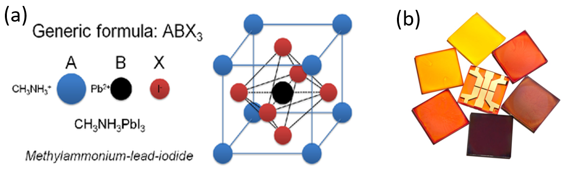
Figure 2: (a) The crystal structure of perovskite semiconductor (b) hybrid perovskite thin films (Plamen Petkov for Scientific American)
Research in the Optoelectronics Group focuses on exploring these new materials and fundamentally understanding how they can efficiently convert light energy into electricity (and the other way around). We work on trying to optimize their performance to produce better light-emitting diodes, solar cells and transistors (did you know there are billions of transistors in a single smartphone?!). We also work on designing controllable functional structures using natural polymers – for example using DNA as a glue to hold small particles together for new applications in batteries and displays. As researchers, we want to ensure that all our processes and fabrication methods are compatible with printing techniques so that we could enable large-scale manufacturing, making the end products as inexpensive as possible.
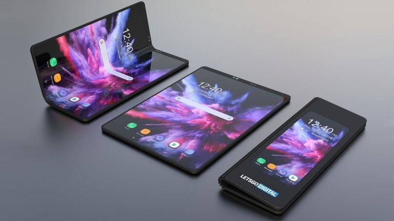
Figure 3: Flexible-display phone (Samsung)
During your visit, we will briefly introduce you to our research areas, ensuring that you will leave with a clear understanding of why and how semiconductor materials emit or absorb light. We will hold an important discussion about how our work will positively impact the world. Climate change is arguably the biggest global challenge our generation faces, and photovoltaics (i.e. solar cells) are a harmless solution to the energy crisis, especially if we want to continue to generate energy at the rate we are currently consuming it. We will also demonstrate to you a handful of state-of-the-art solar cells produced by industrial companies present around our campus. We hope that our work will inspire you to learn more – and to think about the amazing new applications these new devices could open up.
Further Reading
Dr Sam Stranks about perovskites revolutionizing photovoltaics @ TeD 2016
Basic info on the devices we will present (and many others) and the physics behind them can be found on this science and engineering popularizing website: www.howstuffworks.com
You can also check who produces all the novel devices you will experience during your visit to OE group:
Eight19: www.eight19.com